What Role Does Photolithography Play in a Flex PCB Supplier’s Process?
Photolithography is a critical process in the manufacturing of flexible printed circuit boards (flex PCBs), where precision and accuracy are paramount. As flexible electronics continue to grow in popularity, photolithography enables flex PCB suppliers to produce high-quality, reliable circuits that meet the increasing demands of various industries, from consumer electronics to automotive and medical devices. This article explores the essential role of photolithography in the production of flex PCBs, highlighting how flex PCB suppliers leverage this technique to create intricate, high-performance designs.
1. Understanding Photolithography
Photolithography, also known as photomasking or UV lithography, is a process used to transfer a pattern onto a substrate material, such as a flexible plastic film. The process involves using light to expose a photosensitive material (usually a photoresist) on the surface of the substrate. This exposure hardens the photoresist in specific areas, while unexposed areas remain soluble. After developing the photoresist, the substrate is treated with chemicals to etch away the exposed areas, leaving behind precise patterns of conductive traces. This allows flex pcb supplier to create intricate, high-density circuit layouts required for modern electronic devices.
2. Precision and Miniaturization in Flex PCBs
One of the primary challenges in manufacturing flex PCBs is achieving the high precision required for complex and miniature circuit designs. As devices become smaller and more compact, the need for fine-pitch traces and tiny features on PCBs increases. Photolithography enables flex PCB suppliers to produce these small, highly accurate features, including microvias, fine trace lines, and small pads, that are essential for modern electronics. By using advanced photolithography techniques, a flex PCB supplier can maintain tight tolerances and create densely packed, high-performance circuits, even in flexible form factors.
3. Pattern Transfer for Multi-layer Flex Circuits
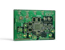
Flex PCBs often consist of multiple layers, each with its own unique pattern of electrical traces. The photolithography process is particularly important when creating multi-layer flex PCBs, as it ensures that the traces and vias align correctly between layers. A flex PCB supplier relies on photolithography to precisely transfer the pattern of each layer onto the flexible substrate. This alignment is crucial for the overall functionality of the PCB, as misalignment can lead to poor electrical performance or even circuit failure. With photolithography, a flex PCB supplier can create multi-layer circuits that are compact, reliable, and capable of handling complex electronic tasks.
4. Improving Circuit Density and Performance
As consumer demand for more powerful and efficient devices continues to grow, circuit density becomes a critical factor in PCB design. Photolithography allows flex PCB suppliers to achieve a high degree of circuit density without sacrificing the board’s flexibility or performance. By precisely etching fine traces and creating microvias, photolithography enables the production of compact and high-density circuits, which is essential for applications such as smartphones, wearables, and medical devices. The ability to integrate more components in a smaller space not only improves the performance of the device but also helps reduce overall size and weight, which are crucial for many flexible electronics applications.
5. Customization of Circuit Patterns
One of the advantages of photolithography is its ability to easily accommodate custom designs. Whether the client requires a unique circuit pattern, specific trace width, or non-standard geometries, photolithography allows for flexible customization. A flex PCB supplier can use photolithography to replicate complex patterns with high accuracy and consistency, providing clients with a fully customized solution. This flexibility is especially important for applications that require specialized layouts, such as flexible antennas, sensors, or circuits that need to conform to particular shapes.
6. Minimizing Defects and Improving Yield Rates
Photolithography also plays a significant role in reducing defects in the manufacturing process. By using precise exposure times and carefully controlled processes, flex PCB suppliers can minimize errors such as overexposure or underexposure of the photoresist, which can result in incomplete or faulty patterns. With the ability to finely control the photolithography process, suppliers can achieve higher yield rates, producing more reliable PCBs and reducing the cost of rework. This ensures that clients receive high-quality, defect-free products on time.
7. Integration with Other Manufacturing Processes
Photolithography is just one step in the broader process of flex PCB fabrication. Once the circuit patterns have been transferred using photolithography, flex PCB suppliers integrate this with other manufacturing processes such as etching, lamination, and component placement. The precise patterns created by photolithography serve as the foundation for these additional steps, ensuring that the final product meets the required specifications. Whether it’s adding soldermask layers, vias, or other components, photolithography helps streamline the overall process and ensures that each step is executed with high precision.
Conclusion
Photolithography is a cornerstone of flex PCB suppliers’ manufacturing processes, enabling them to create precise, reliable, and high-performance flexible printed circuit boards. From enhancing circuit density to supporting multi-layer designs and custom patterns, photolithography allows flex PCB suppliers to meet the unique demands of various industries. By leveraging this advanced technique, suppliers can ensure that their flex PCBs are capable of powering the next generation of compact, efficient, and durable electronic devices.