
Prototype Circuit Board Assembly
The layer count in a prototype circuit board assembly is a crucial factor when choosing the correct design. It determines signal integrity, component placement, and how much space is available for routing connections. Higher layer counts offer more options for shielding, controlled impedance routing, and power/ground plane placement, reducing crosstalk and EMI. However, they also introduce additional manufacturing complexity and cost. This article will explore the ideal layer counts, layout conventions, and considerations for designing a multilayer PCB.
The PCB’s core is made up of the copper traces that connect components and route signals. They are typically separated by ground and power layers, which help protect against static electricity and maintain consistent conductivity throughout the board. These layers are also used to ensure that the traces don’t cross each other, protecting against shorts and potential damage to the circuit.
Routing layers contain the copper traces that connect components on the surface and inner sides of the PCB. These traces carry digital and analog signals, as well as power and ground connections. They can be arranged in a variety of configurations, depending on the needs of the circuit design. For example, high-speed designs may require more signal layers to support faster data transmission. Meanwhile, lower-pin-count complex devices with lower signal integrity requirements may need fewer signal layers.
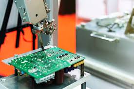
Layer Counts in a Prototype Circuit Board Assembly
A prepreg layer is a dielectric material that provides insulation between the conductive copper layers and ensures proper adhesion during lamination. It’s also responsible for filling in and smoothing out any surface irregularities on the copper layers. The amount of prepreg used affects the overall thickness of the finished board.
The silkscreen layer is a graphical overlay that includes important information for the assembly, testing, and maintenance of a PCB. It includes component designations, pin 1 indicators, polarity indicators, and test points, as well as the manufacturer’s logo and revision number. It’s also essential for performing visual and X-ray inspections of the board.
While thicker PCBs can improve thermal management, this is mainly achieved through the use of copper pours and blind vias. In general, a higher layer count doesn’t necessarily improve thermal performance, and a focus on good design and materials is more effective. In this article, we will dive into the details of prototype circuit board assembly, including the process, key considerations, challenges, and best practices for building an effective and reliable prototype.
A prototype circuit board assembly (PCBA) is an essential step in the development of electronic devices. It allows engineers and designers to test and verify the functionality of their designs before moving to large-scale production. A PCBA typically includes the printed circuit board (PCB) with all its components soldered onto it, creating a fully functional circuit. Prototyping provides critical insights into how the design performs in real-world conditions and helps identify potential issues early in the development process, saving both time and money.